Introduction
I recently purchased the Digilent Analog Discovery (Revision C). In this post I am looking at the Digital features, in particular the Pattern Generator and Logic Analyzer functionality.
Test Circuit Setup
For this test circuit I am going to use a JK Flip-Flop, in this case a negative-edge triggered JK Flip-Flop, the 74HCT112N, which is manufactured by NXP/Philips. Like all JK Flip-Flops, it has the very useful property that when both J and K inputs are set high that the flip-flop goes in to a ‘toggle’ state, where the Q outputs will switch from high->low and low->high repeatedly whenever a full clock cycle is applied. This means that Q will toggle at half the frequency of the clock pulse.
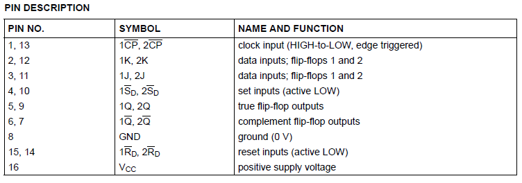
From the datasheet table below you can see the pin setup of the 74HCT112. The first thing to note is that this flip-flop is a negative-edge triggered flip-flop – you can see this as there is a bar over the CP input on pin 1. The next think is that there is a SET input, which is active low, to asynchronously set the flip-flop to store a high (i.e. Q=1) and a RESET input which will set the flip-flop to store a low (i.e. Q=0). As these inputs are both active-low inputs I would like to tie them high (so, pins 4 & 15 high).
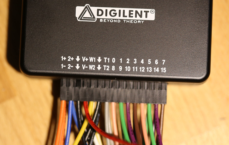
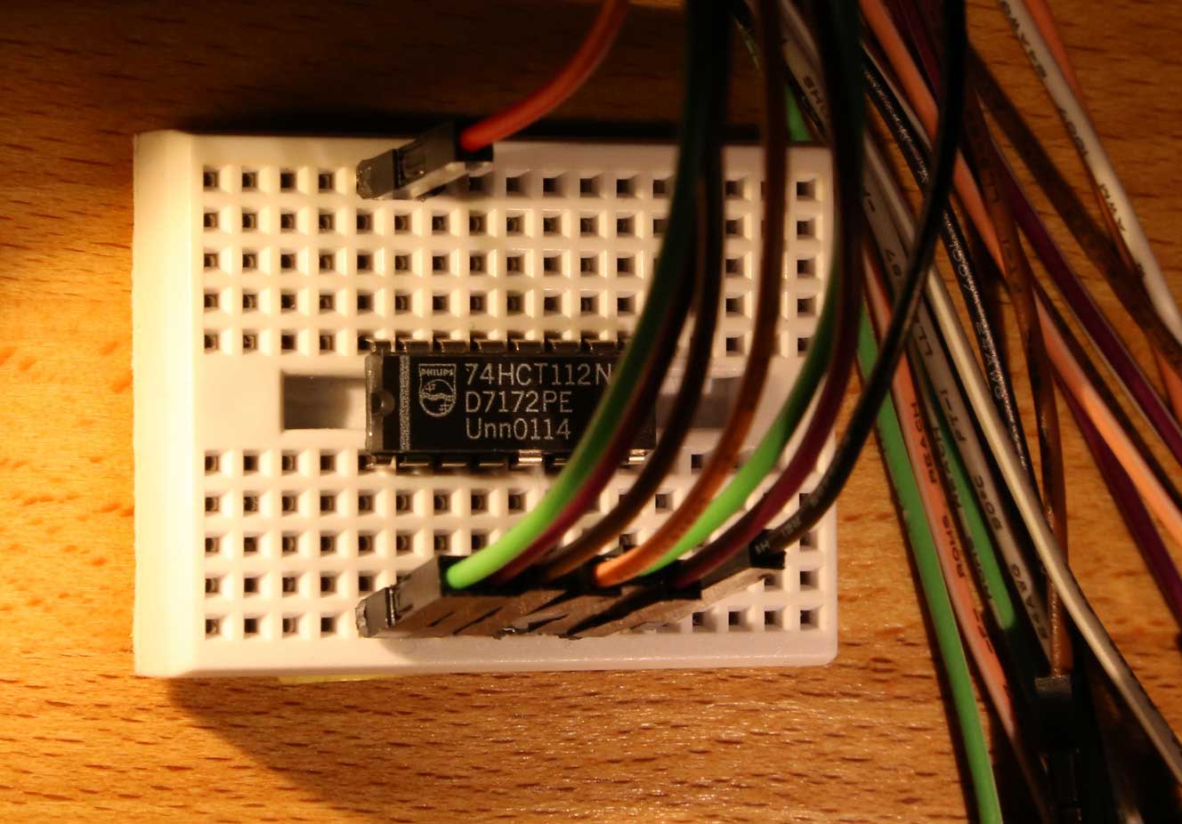
I have wired the circuit as captured in Figure 1. You can see the leads going from the Analog Discovery into the small breadboard. I have used the same input/output numbers as the chip, so for example, I used discovery input/output 1 to connect to pin 1 of the chip and so on. Pins 1, 2, 3, 4, and 15 are outputs to the chip and Pins 5 and 6 are inputs from the chip.
Figure 1. The Wiring of my Circuit
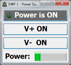
I have wired V+ from the Analog Discovery to the Vcc input of the JK flip-flop on pin 16 and one of the GND values on the Analog Discovery (a down arrow) to the GND input of the JK flip-flop on pin 8. After everything was wired, I was able to power the chip using the discovery using the Power Supply Window (as captured in Figure 2.). This function has short-circuit protection and also gives a useful indication of the power delivered and available. In Figure 2 the power supply is now on.
Figure 2. The Power Supply Window
The Pattern Generator
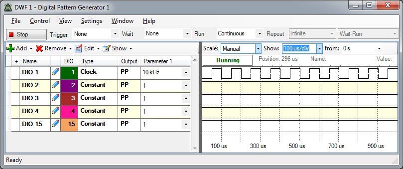
Now, I must set up the outputs to the JK flip-flop using the Digital Pattern Generator Window as illustrated in Figure 3. I have set all of the outputs to be PP (Push Pull) values, where the allowable values are 0 or 1.
- DIO1 is set to a Clock output and connected to the CLK input of the flip-flop (chip pin 1)
- DIO2 is set to a high output and connected to K (pin 2)
- DIO3 is set to a high output and connected to J (pin 3)
- DIO4 is set to a high output and connected to the asynchronous set inputs /Sd (pin 4) so this is deactivated
- DIO15 is set to a high output and connected to the asynchronous reset inputs /Rd (pin 15) so this is deactivated.
Once this is ready we can hit the Run button to run the signals to the JK flip-flop IC.
Figure 3. The Digital Pattern Generator Window
The Logic Analyzer
Next, we want to read the values. Here I have set up the inputs as follows:
- DIO5 is connected to the Q output of the JK flip-flop (chip pin 5)
- DIO6 is connected to the /Q output of the JK flip-flop (chip pin 6)
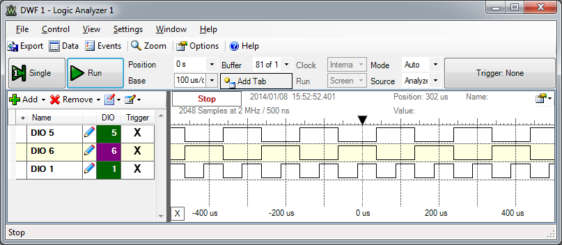
- DIO1 is the clock output as set by the Pattern Generator in Figure 3; however, we would like to synchronize this with our output values for Q and /Q so that we can compare the signals.
Once you are ready you can hit the Run button. There is no need to set a trigger.
Figure 4. The Logic Analyzer Window
Figure 4, captures the results and you can see it is exactly as I would expect. The frequency of the Q and /Q are exactly half that of the clock inputs. They are synchronized, with the Q and /Q values changing on the falling edge of the clock signal. You can change the frequency of the clock signal and you can see the impact of this on the outputs using the Logic Analyzer.
The Static I/O Window
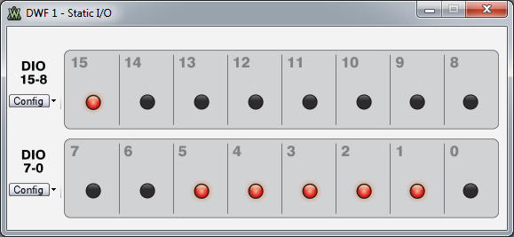
If you set the clock frequency to be low you can also use the Static I/O Window to view the outputs. You will see the virtual LEDs flashing in Figure 5.
Figure 5. The Static I/O Window
Observations and Conclusions
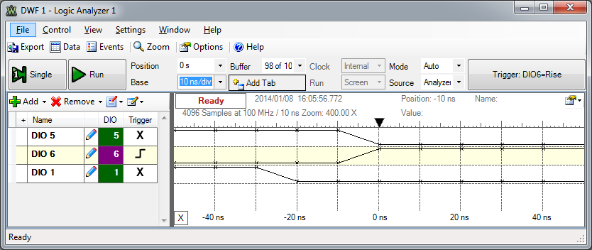
Finally, I have changed the base to 10ns/div and used a trigger on the rising edge of /Q (same as falling edge of Q). You can see this on the right-hand side where I have set “Trigger: DIO6=Rise”. You can see here that the propagation delay of this JK Flip-Flop is about 20ns – this is the time it takes for the output to change according to the newly applied inputs. This measured value concurs with the data sheet, which states that the propagation delay from n/CP to nQ is 19ns for the HCT version of this chip.
Figure 6. The Logic Analyzer Window with a time base of 10 nanoseconds per division.
So, The Analog Discovery is not only very useful for generating and measuring analog signals, it is also very useful for looking at the ‘digital’ response of digital circuits. I have only scratched the surface of the digital functionality of the Analog Discovery. The significant benefits arise when you connect the Discovery to a bus, enabling you to decode the data on the bus into human readable form.
In conclusion, the functionality of the Analog Discovery is very impressive, especially as an education tool, for the price point of $99 for a US Student or $219 for the non-student version.



Given article is very helpful and very useful for my admin, and pardon me permission to share articles here hopefully helped.